Key Steps in Prototype Circuit Board Assembly
The first step is to prepare the bare PCB panel. This involves printing a set of Gerber files that describe the PCB layout. These files are generated from the CAD software used to create the circuit board design. Depending on the prototyping method chosen, the bare board can be made with one or two layers. The CAD files also contain a bill of materials that the manufacturer uses to order the required components for each layer of the PCB.
Once the bare panel has been prepared, holes are drilled at the locations specified in the design. The size and depth of the holes depends on the component specifications. A copper layer is then applied to the panel. This is done using a chemical bath. Once the copper has been applied, the board is imaged with another set of files, known as the manufacturing file. The PCB fabrication process then begins.
During this process, the copper is pre-bonded to the substrate material. Then the boards are coated in a solder mask, which protects all but the areas that will be soldered. The next step is to print the solder paste. A stencil is then placed on the board, and the paste is squeegeed onto each pad in the correct location. The solder paste is then melted through a process called reflow.
What Are the Key Steps in Prototype Circuit Board Assembly?
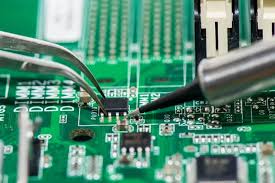
Next, the components are placed on the prototype circuit board assembly. This is usually done by hand by experienced engineering staff. The engineers use the client’s PCB design files to correctly place the components on the corresponding positions of the board. This is a very important step and requires great skill to achieve the high quality that MPL is famous for.
The engineering staff must ensure that the components are correctly oriented and that they adhere to all regulations and operation standards of thru-hole mounting processes. The engineering team must also be aware of the polarity of the components, and they must wear anti-static wristbands to avoid damaging the delicate components.
After the component placement is complete, the populated PCBs are sent through a final inspection process called AOI or AXI (Automated Optical Inspection and Automated X-Ray Inspection). The machines make a series of visual checks on the assembles to verify that all components have been correctly positioned. The AOI and AXI tests also look for any errors that could have occurred during the component placement or the reflow soldering process.
If the AOI and AXI results are satisfactory, then the final step of PCB assembly is to test each assemble for functionality by putting it through power and simulated signals. If it fails, then the assemble is scrapped and recycled. This is why regular testing and inspection throughout the process is so important. It allows any issues to be spotted early and rectified before they cause costly delays in production. If you need to get a prototype circuit board assembled quickly and accurately, please contact MPL.